|
coreboot
coreboot is an Open Source project aimed at replacing the proprietary BIOS found in most computers.
|
|
coreboot
coreboot is an Open Source project aimed at replacing the proprietary BIOS found in most computers.
|
#include <acpi/acpi.h>
Go to the source code of this file.
Data Structures | |
| struct | chipset_power_state |
Macros | |
| #define | IOCOM1 0x3f8 |
| #define | PRSTS 0x00 |
| #define | PMC_WDT_STS (1 << 15) |
| #define | SEC_GBLRST_STS (1 << 7) |
| #define | SEC_WDT_STS (1 << 6) |
| #define | WOL_OVR_WK_STS (1 << 5) |
| #define | PMC_WAKE_STS (1 << 4) |
| #define | PMC_CFG 0x08 |
| #define | SPS (1 << 5) |
| #define | NO_REBOOT (1 << 4) |
| #define | SX_ENT_TO_EN (1 << 3) |
| #define | TIMING_T581_SHIFT (0) |
| #define | TIMING_T581_MASK (3 << TIMING_T581_SHIFT) |
| #define | TIMING_T581_10uS (0 << TIMING_T581_SHIFT) |
| #define | TIMING_T581_100uS (1 << TIMING_T581_SHIFT) |
| #define | TIMING_T581_1mS (2 << TIMING_T581_SHIFT) |
| #define | TIMING_T581_10mS (3 << TIMING_T581_SHIFT) |
| #define | VLV_PM_STS 0x0c |
| #define | PMC_MSG_FULL_STS (1 << 24) |
| #define | PMC_MSG_4_FULL_STS (1 << 23) |
| #define | PMC_MSG_3_FULL_STS (1 << 22) |
| #define | PMC_MSG_2_FULL_STS (1 << 21) |
| #define | PMC_MSG_1_FULL_STS (1 << 20) |
| #define | CODE_REQ (1 << 8) |
| #define | HPR_ENT_TO (1 << 2) |
| #define | SX_ENT_TO (1 << 1) |
| #define | GEN_PMCON1 0x20 |
| #define | UART_EN (1 << 24) |
| #define | DISB (1 << 23) |
| #define | MEM_SR (1 << 21) |
| #define | SRS (1 << 20) |
| #define | CTS (1 << 19) |
| #define | MS4V (1 << 18) |
| #define | PWR_FLR (1 << 16) |
| #define | PME_B0_S5_DIS (1 << 15) |
| #define | SUS_PWR_FLR (1 << 14) |
| #define | WOL_EN_OVRD (1 << 13) |
| #define | DIS_SLP_X_STRCH_SUS_UP (1 << 12) |
| #define | GEN_RST_STS (1 << 9) |
| #define | RPS (1 << 2) |
| #define | AFTERG3_EN (1 << 0) |
| #define | GEN_PMCON2 0x24 |
| #define | SLPSX_STR_POL_LOCK (1 << 18) |
| #define | BIOS_PCI_EXP_EN (1 << 10) |
| #define | PWRBTN_LVL (1 << 9) |
| #define | SMI_LOCK (1 << 4) |
| #define | ETR 0x48 |
| #define | CF9LOCK (1 << 31) |
| #define | LTR_DEF (1 << 22) |
| #define | IGNORE_HPET (1 << 21) |
| #define | CF9GR (1 << 20) |
| #define | CWORWRE (1 << 18) |
| #define | FUNC_DIS 0x34 |
| #define | SIO_DMA2_DIS (1 << 0) |
| #define | PWM1_DIS (1 << 1) |
| #define | PWM2_DIS (1 << 2) |
| #define | HSUART1_DIS (1 << 3) |
| #define | HSUART2_DIS (1 << 4) |
| #define | SPI_DIS (1 << 5) |
| #define | SDIO_DIS (1 << 9) |
| #define | SD_DIS (1 << 10) |
| #define | MMC_DIS (1 << 11) |
| #define | HDA_DIS (1 << 12) |
| #define | LPE_DIS (1 << 13) |
| #define | OTG_DIS (1 << 14) |
| #define | XHCI_DIS (1 << 15) |
| #define | SATA_DIS (1 << 17) |
| #define | EHCI_DIS (1 << 18) |
| #define | TXE_DIS (1 << 19) |
| #define | PCIE_PORT1_DIS (1 << 20) |
| #define | PCIE_PORT2_DIS (1 << 21) |
| #define | PCIE_PORT3_DIS (1 << 22) |
| #define | PCIE_PORT4_DIS (1 << 23) |
| #define | SIO_DMA1_DIS (1 << 24) |
| #define | I2C1_DIS (1 << 25) |
| #define | I2C2_DIS (1 << 26) |
| #define | I2C3_DIS (1 << 27) |
| #define | I2C4_DIS (1 << 28) |
| #define | I2C5_DIS (1 << 29) |
| #define | I2C6_DIS (1 << 30) |
| #define | I2C7_DIS (1 << 31) |
| #define | FUNC_DIS2 0x38 |
| #define | USH_SS_PHY_DIS (1 << 2) |
| #define | OTG_SS_PHY_DIS (1 << 1) |
| #define | SMBUS_DIS (1 << 0) |
| #define | GPIO_ROUT 0x58 |
| #define | ROUTE_MASK 3 |
| #define | ROUTE_NONE 0 |
| #define | ROUTE_SMI 1 |
| #define | ROUTE_SCI 2 |
| #define | PLT_CLK_CTL_0 0x60 |
| #define | PLT_CLK_CTL_1 0x64 |
| #define | PLT_CLK_CTL_2 0x68 |
| #define | PLT_CLK_CTL_3 0x6c |
| #define | PLT_CLK_CTL_4 0x70 |
| #define | PLT_CLK_CTL_5 0x74 |
| #define | CLK_SRC_XTAL (0x0 << 2) |
| #define | CLK_SRC_PLL (0x1 << 2) |
| #define | CLK_CTL_D3_LPE (0x0 << 0) |
| #define | CLK_CTL_ON (0x1 << 0) |
| #define | CLK_CTL_OFF (0x2 << 0) |
| #define | PME_STS 0xc0 |
| #define | GPE_LEVEL_EDGE 0xc4 |
| #define | GPE_EDGE 0 |
| #define | GPE_LEVEL 1 |
| #define | GPE_POLARITY 0xc8 |
| #define | GPE_ACTIVE_HIGH 1 |
| #define | GPE_ACTIVE_LOW 0 |
| #define | LOCK 0xcc |
| #define | PM1_STS 0x00 |
| #define | WAK_STS (1 << 15) |
| #define | PCIEXPWAK_STS (1 << 14) |
| #define | USB_STS (1 << 13) |
| #define | PRBTNOR_STS (1 << 11) |
| #define | RTC_STS (1 << 10) |
| #define | PWRBTN_STS (1 << 8) |
| #define | GBL_STS (1 << 5) |
| #define | TMROF_STS (1 << 0) |
| #define | PM1_EN 0x02 |
| #define | PCIEXPWAK_DIS (1 << 14) |
| #define | USB_WAKE_EN (1 << 13) |
| #define | RTC_EN (1 << 10) |
| #define | PWRBTN_EN (1 << 8) |
| #define | GBL_EN (1 << 5) |
| #define | TMROF_EN (1 << 0) |
| #define | PM1_CNT 0x04 |
| #define | GBL_RLS (1 << 2) |
| #define | BM_RLD (1 << 1) |
| #define | SCI_EN (1 << 0) |
| #define | PM1_TMR 0x08 |
| #define | GPE0_STS 0x20 |
| #define | GPE0_EN 0x28 |
| #define | SUS_GPIO_EN7_BIT 23 |
| #define | SUS_GPIO_EN7 (1 << SUS_GPIO_EN7_BIT) |
| #define | SUS_GPIO_EN6_BIT 22 |
| #define | SUS_GPIO_EN6 (1 << SUS_GPIO_EN6_BIT) |
| #define | SUS_GPIO_EN5_BIT 21 |
| #define | SUS_GPIO_EN5 (1 << SUS_GPIO_EN5_BIT) |
| #define | SUS_GPIO_EN4_BIT 20 |
| #define | SUS_GPIO_EN4 (1 << SUS_GPIO_EN4_BIT) |
| #define | SUS_GPIO_EN3_BIT 19 |
| #define | SUS_GPIO_EN3 (1 << SUS_GPIO_EN3_BIT) |
| #define | SUS_GPIO_EN2_BIT 18 |
| #define | SUS_GPIO_EN2 (1 << SUS_GPIO_EN2_BIT) |
| #define | SUS_GPIO_EN1_BIT 17 |
| #define | SUS_GPIO_EN1 (1 << SUS_GPIO_EN1_BIT) |
| #define | SUS_GPIO_EN0_BIT 16 |
| #define | SUS_GPIO_EN0 (1 << SUS_GPIO_EN0_BIT) |
| #define | SUS_GPIO_STS0 (1 << 16) |
| #define | PCIE_WAKE3_STS (1 << 8) |
| #define | PCIE_WAKE2_STS (1 << 7) |
| #define | PCIE_WAKE1_STS (1 << 6) |
| #define | PCIE_WAKE0_STS (1 << 3) |
| #define | PCI_EXP_STS (1 << 9) |
| #define | PME_B0_EN (1 << 13) |
| #define | _ACPI_ENABLE_WAKE_SUS_GPIO(x) SUS_GPIO_EN##x##_BIT |
| #define | ACPI_ENABLE_WAKE_SUS_GPIO(x) _ACPI_ENABLE_WAKE_SUS_GPIO(x) |
| #define | SMI_EN 0x30 |
| #define | INTEL_USB2_EN (1 << 18) /* Intel-Specific USB2 SMI logic */ |
| #define | USB_EN (1 << 17) /* Legacy USB2 SMI logic */ |
| #define | PERIODIC_EN (1 << 14) /* SMI on PERIODIC_STS in SMI_STS */ |
| #define | TCO_EN (1 << 13) /* Enable TCO Logic (BIOSWE et al) */ |
| #define | BIOS_RLS (1 << 7) /* asserts SCI on bit set */ |
| #define | SWSMI_TMR_EN (1 << 6) /* start software smi timer on bit set */ |
| #define | APMC_EN (1 << 5) /* Writes to APM_CNT cause SMI# */ |
| #define | SLP_SMI_EN (1 << 4) /* Write to SLP_EN in PM1_CNT asserts SMI# */ |
| #define | BIOS_EN (1 << 2) /* Assert SMI# on setting GBL_RLS bit */ |
| #define | EOS (1 << 1) /* End of SMI (deassert SMI#) */ |
| #define | GBL_SMI_EN (1 << 0) /* SMI# generation at all? */ |
| #define | SMI_STS 0x34 |
| #define | ALT_GPIO_SMI 0x38 |
| #define | UPRWC 0x3c |
| #define | UPRWC_WR_EN (1 << 1) /* USB Per-Port Registers Write Enable */ |
| #define | GPE_CTRL 0x40 |
| #define | PM2A_CNT_BLK 0x50 |
| #define | TCO_RLD 0x60 |
| #define | TCO_STS 0x64 |
| #define | SECOND_TO_STS (1 << 17) |
| #define | TCO_TIMEOUT (1 << 3) |
| #define | TCO1_CNT 0x68 |
| #define | TCO_LOCK (1 << 12) |
| #define | TCO_TMR_HALT (1 << 11) |
| #define | TCO_TMR 0x70 |
Functions | |
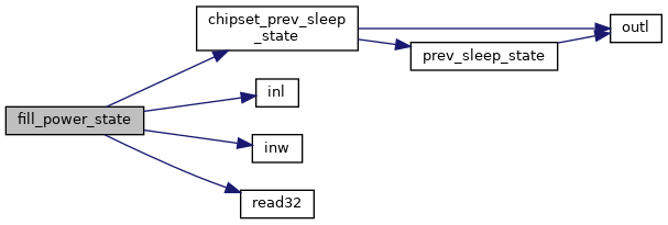
| struct chipset_power_state * | fill_power_state (void) |
| uint16_t | get_pmbase (void) |
| uint32_t | clear_smi_status (void) |
| uint16_t | clear_pm1_status (void) |
| uint32_t | clear_tco_status (void) |
| uint32_t | clear_gpe_status (void) |
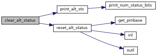
| uint32_t | clear_alt_status (void) |
| void | clear_pmc_status (void) |
| void | enable_smi (uint32_t mask) |
| void | disable_smi (uint32_t mask) |
| void | enable_pm1 (uint16_t events) |
| void | enable_pm1_control (uint32_t mask) |
| void | disable_pm1_control (uint32_t mask) |
| void | enable_gpe (uint32_t mask) |
| void | disable_gpe (uint32_t mask) |
| void | disable_all_gpe (void) |
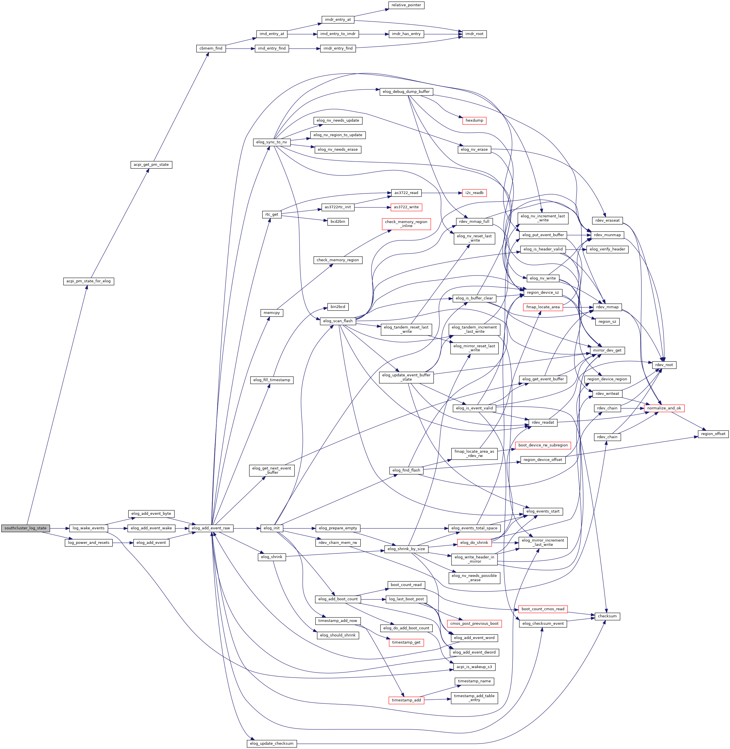
| void | southcluster_log_state (void) |
| int | rtc_failure (void) |
Variables | |
| struct chipset_power_state | __packed |
| #define ACPI_ENABLE_WAKE_SUS_GPIO | ( | x | ) | _ACPI_ENABLE_WAKE_SUS_GPIO(x) |
| #define INTEL_USB2_EN (1 << 18) /* Intel-Specific USB2 SMI logic */ |
| #define SUS_GPIO_EN0 (1 << SUS_GPIO_EN0_BIT) |
| #define SUS_GPIO_EN1 (1 << SUS_GPIO_EN1_BIT) |
| #define SUS_GPIO_EN2 (1 << SUS_GPIO_EN2_BIT) |
| #define SUS_GPIO_EN3 (1 << SUS_GPIO_EN3_BIT) |
| #define SUS_GPIO_EN4 (1 << SUS_GPIO_EN4_BIT) |
| #define SUS_GPIO_EN5 (1 << SUS_GPIO_EN5_BIT) |
| #define SUS_GPIO_EN6 (1 << SUS_GPIO_EN6_BIT) |
| #define SUS_GPIO_EN7 (1 << SUS_GPIO_EN7_BIT) |
| #define SWSMI_TMR_EN (1 << 6) /* start software smi timer on bit set */ |
| #define TIMING_T581_100uS (1 << TIMING_T581_SHIFT) |
| #define TIMING_T581_10mS (3 << TIMING_T581_SHIFT) |
| #define TIMING_T581_10uS (0 << TIMING_T581_SHIFT) |
| #define TIMING_T581_1mS (2 << TIMING_T581_SHIFT) |
| #define TIMING_T581_MASK (3 << TIMING_T581_SHIFT) |
| #define UPRWC_WR_EN (1 << 1) /* USB Per-Port Registers Write Enable */ |
Definition at line 312 of file pmutil.c.
References print_alt_sts(), and reset_alt_status().
| struct chipset_power_state* fill_power_state | ( | void | ) |
Definition at line 31 of file romstage.c.
References ACPI_BASE_ADDRESS, BIOS_DEBUG, chipset_prev_sleep_state(), GEN_PMCON1, chipset_power_state::gen_pmcon1, GEN_PMCON2, chipset_power_state::gen_pmcon2, GPE0_EN, chipset_power_state::gpe0_en, GPE0_STS, chipset_power_state::gpe0_sts, inl(), inw(), PM1_CNT, chipset_power_state::pm1_cnt, PM1_EN, chipset_power_state::pm1_en, PM1_STS, chipset_power_state::pm1_sts, PMC_BASE_ADDRESS, power_state, chipset_power_state::prev_sleep_state, printk, PRSTS, chipset_power_state::prsts, read32(), TCO_STS, and chipset_power_state::tco_sts.
Definition at line 76 of file elog.c.
References acpi_pm_state_for_elog(), log_power_and_resets(), and log_wake_events().
Referenced by smm_southbridge_clear_state().

| struct chipset_power_state __packed |