|
coreboot
coreboot is an Open Source project aimed at replacing the proprietary BIOS found in most computers.
|
|
coreboot
coreboot is an Open Source project aimed at replacing the proprietary BIOS found in most computers.
|
#include <stdint.h>#include "memmap.h"#include <northbridge/intel/common/fixed_bars.h>#include <device/device.h>

Go to the source code of this file.
Data Structures | |
| struct | timings_t |
| struct | dimminfo_t |
| struct | sysinfo_t |
| struct | blc_pwm_t |
Macros | |
| #define | TOTAL_CHANNELS 2 |
| #define | CHANNEL_IS_POPULATED(dimms, idx) (dimms[idx].card_type != 0) |
| #define | CHANNEL_IS_CARDF(dimms, idx) (dimms[idx].card_type == 0xf) |
| #define | IF_CHANNEL_POPULATED(dimms, idx) if (dimms[idx].card_type != 0) |
| #define | FOR_EACH_CHANNEL(idx) for (idx = 0; idx < TOTAL_CHANNELS; ++idx) |
| #define | FOR_EACH_POPULATED_CHANNEL(dimms, idx) FOR_EACH_CHANNEL(idx) IF_CHANNEL_POPULATED(dimms, idx) |
| #define | RANKS_PER_CHANNEL 4 /* Only two may be populated */ |
| #define | IF_RANK_POPULATED(dimms, ch, r) if (dimms[ch].card_type && ((r) < dimms[ch].ranks)) |
| #define | FOR_EACH_RANK_IN_CHANNEL(r) for (r = 0; r < RANKS_PER_CHANNEL; ++r) |
| #define | FOR_EACH_POPULATED_RANK_IN_CHANNEL(dimms, ch, r) FOR_EACH_RANK_IN_CHANNEL(r) IF_RANK_POPULATED(dimms, ch, r) |
| #define | FOR_EACH_RANK(ch, r) FOR_EACH_CHANNEL(ch) FOR_EACH_RANK_IN_CHANNEL(r) |
| #define | FOR_EACH_POPULATED_RANK(dimms, ch, r) FOR_EACH_RANK(ch, r) IF_RANK_POPULATED(dimms, ch, r) |
| #define | DDR3_MAX_CAS 18 |
| #define | CMOS_READ_TRAINING 0x80 /* 16 bytes */ |
| #define | CMOS_WRITE_TRAINING 0x90 /* 16 bytes (could be reduced to 10 bytes) */ |
| #define | D0F0_EPBAR_LO 0x40 |
| #define | D0F0_EPBAR_HI 0x44 |
| #define | D0F0_MCHBAR_LO 0x48 |
| #define | D0F0_MCHBAR_HI 0x4c |
| #define | D0F0_GGC 0x52 |
| #define | D0F0_DEVEN 0x54 |
| #define | D0F0_PCIEXBAR_LO 0x60 |
| #define | D0F0_PCIEXBAR_HI 0x64 |
| #define | D0F0_DMIBAR_LO 0x68 |
| #define | D0F0_DMIBAR_HI 0x6c |
| #define | D0F0_PMBASE 0x78 |
| #define | D0F0_PAM(x) (0x90 + (x)) /* 0-6 */ |
| #define | D0F0_REMAPBASE 0x98 |
| #define | D0F0_REMAPLIMIT 0x9a |
| #define | D0F0_SMRAM 0x9d |
| #define | D0F0_ESMRAMC 0x9e |
| #define | D0F0_TOM 0xa0 |
| #define | D0F0_TOUUD 0xa2 |
| #define | D0F0_TOLUD 0xb0 |
| #define | D0F0_SKPD 0xdc /* Scratchpad Data */ |
| #define | D0F0_CAPID0 0xe0 |
| #define | PEG_CAP 0xa2 |
| #define | SLOTCAP 0xb4 |
| #define | PEGLC 0xec |
| #define | D1F0_VCCAP 0x104 |
| #define | D1F0_VC0RCTL 0x114 |
| #define | GCFGC_PCIDEV PCI_DEV(0, 2, 0) |
| #define | GCFGC_OFFSET 0xf0 |
| #define | GCFGC_CR_SHIFT 0 |
| #define | GCFGC_CR_MASK (0xf << GCFGC_CR_SHIFT) |
| #define | GCFGC_CS_SHIFT 8 |
| #define | GCFGC_CS_MASK (0xf << GCFGC_CS_SHIFT) |
| #define | GCFGC_CD_SHIFT 12 |
| #define | GCFGC_CD_MASK (0x1 << GCFGC_CD_SHIFT) |
| #define | GCFGC_UPDATE_SHIFT 5 |
| #define | GCFGC_UPDATE (0x1 << GCFGC_UPDATE_SHIFT) |
| #define | HPLLVCO_MCHBAR 0x0c0f |
| #define | PMSTS_MCHBAR 0x0f14 /* Self refresh channel status */ |
| #define | PMSTS_WARM_RESET (1 << 1) |
| #define | PMSTS_BOTH_SELFREFRESH (1 << 0) |
| #define | CLKCFG_MCHBAR 0x0c00 |
| #define | CLKCFG_FSBCLK_SHIFT 0 |
| #define | CLKCFG_FSBCLK_MASK (7 << CLKCFG_FSBCLK_SHIFT) |
| #define | CLKCFG_MEMCLK_SHIFT 4 |
| #define | CLKCFG_MEMCLK_MASK (7 << CLKCFG_MEMCLK_SHIFT) |
| #define | CLKCFG_UPDATE (1 << 12) |
| #define | SSKPD_MCHBAR 0x0c1c |
| #define | SSKPD_CLK_SHIFT 0 |
| #define | SSKPD_CLK_MASK (7 << SSKPD_CLK_SHIFT) |
| #define | DCC_MCHBAR 0x200 |
| #define | DCC_NO_CHANXOR (1 << 10) |
| #define | DCC_INTERLEAVED (1 << 1) |
| #define | DCC_CMD_SHIFT 16 |
| #define | DCC_CMD_MASK (7 << DCC_CMD_SHIFT) |
| #define | DCC_CMD_NOP (1 << DCC_CMD_SHIFT) |
| #define | DCC_SET_MREG (3 << DCC_CMD_SHIFT) |
| #define | DCC_SET_EREG (4 << DCC_CMD_SHIFT) |
| #define | DCC_SET_EREG_SHIFT 21 |
| #define | DCC_SET_EREG_MASK (DCC_CMD_MASK | (3 << DCC_SET_EREG_SHIFT)) |
| #define | DCC_SET_EREGx(x) |
| #define | CxDRA_MCHBAR(x) (0x1208 + ((x) * 0x0100)) |
| #define | CxDRA_PAGESIZE_SHIFT(r) ((r) * 4) /* Per rank r */ |
| #define | CxDRA_PAGESIZE_MASKr(r) (0x7 << CxDRA_PAGESIZE_SHIFT(r)) |
| #define | CxDRA_PAGESIZE_MASK 0x0000ffff |
| #define | CxDRA_PAGESIZE(r, p) |
| #define | CxDRA_BANKS_SHIFT(r) (((r) * 3) + 16) |
| #define | CxDRA_BANKS_MASKr(r) (0x3 << CxDRA_BANKS_SHIFT(r)) |
| #define | CxDRA_BANKS_MASK 0x07ff0000 |
| #define | CxDRA_BANKS(r, b) |
| #define | CxDRBy_MCHBAR(x, r) (0x1200 + ((x) * 0x0100) + (((r) / 2) * 4)) |
| #define | CxDRBy_BOUND_SHIFT(r) (((r) % 2) * 16) |
| #define | CxDRBy_BOUND_MASK(r) (0x1fc << CxDRBy_BOUND_SHIFT(r)) |
| #define | CxDRBy_BOUND_MB(r, b) |
| #define | CxDRC0_MCHBAR(x) (0x1230 + ((x) * 0x0100)) |
| #define | CxDRC0_RANKEN0 (1 << 24) /* Rank Enable */ |
| #define | CxDRC0_RANKEN1 (1 << 25) |
| #define | CxDRC0_RANKEN2 (1 << 26) |
| #define | CxDRC0_RANKEN3 (1 << 27) |
| #define | CxDRC0_RANKEN(r) (1 << (24 + (r))) |
| #define | CxDRC0_RANKEN_MASK (0xf << 24) |
| #define | CxDRC0_RMS_SHIFT 8 /* Refresh Mode Select */ |
| #define | CxDRC0_RMS_MASK (7 << CxDRC0_RMS_SHIFT) |
| #define | CxDRC0_RMS_78US (2 << CxDRC0_RMS_SHIFT) |
| #define | CxDRC0_RMS_39US (3 << CxDRC0_RMS_SHIFT) |
| #define | CxDRC1_MCHBAR(x) (0x1234 + ((x) * 0x0100)) |
| #define | CxDRC1_SSDS_SHIFT 24 |
| #define | CxDRC1_SSDS_MASK (0xff << CxDRC1_SSDS_SHIFT) |
| #define | CxDRC1_DS (0x91 << CxDRC1_SSDS_SHIFT) |
| #define | CxDRC1_SS (0xb1 << CxDRC1_SSDS_SHIFT) |
| #define | CxDRC1_NOTPOP(r) (1 << (16 + (r))) /* Write 1 for Not Populated */ |
| #define | CxDRC1_NOTPOP_MASK (0xf << 16) |
| #define | CxDRC1_MUSTWR (3 << 11) |
| #define | CxDRC2_MCHBAR(x) (0x1238 + ((x) * 0x0100)) |
| #define | CxDRC2_NOTPOP(r) (1 << (24 + (r))) /* Write 1 for Not Populated */ |
| #define | CxDRC2_NOTPOP_MASK (0xf << 24) |
| #define | CxDRC2_MUSTWR (1 << 12) |
| #define | CxDRC2_CLK1067MT (1 << 0) |
| #define | CxDRT0_MCHBAR(x) (0x1210 + ((x) * 0x0100)) |
| #define | CxDRT0_BtB_WtP_SHIFT 26 |
| #define | CxDRT0_BtB_WtP_MASK (0x1f << CxDRT0_BtB_WtP_SHIFT) |
| #define | CxDRT0_BtB_WtR_SHIFT 20 |
| #define | CxDRT0_BtB_WtR_MASK (0x1f << CxDRT0_BtB_WtR_SHIFT) |
| #define | CxDRT1_MCHBAR(x) (0x1214 + ((x) * 0x0100)) |
| #define | CxDRT2_MCHBAR(x) (0x1218 + ((x) * 0x0100)) |
| #define | CxDRT3_MCHBAR(x) (0x121c + ((x) * 0x0100)) |
| #define | CxDRT4_MCHBAR(x) (0x1220 + ((x) * 0x0100)) |
| #define | CxDRT5_MCHBAR(x) (0x1224 + ((x) * 0x0100)) |
| #define | CxDRT6_MCHBAR(x) (0x1228 + ((x) * 0x0100)) |
| #define | CxDCLKDIS_MCHBAR(x) (0x120c + ((x) * 0x0100)) |
| #define | CxDCLKDIS_MASK 3 |
| #define | CxDCLKDIS_ENABLE 3 /* Always enable both clock pairs. */ |
| #define | CxODT_HIGH(x) (0x124c + ((x) * 0x0100)) |
| #define | CxODT_LOW(x) (0x1248 + ((x) * 0x0100)) |
| #define | CxWRTy_MCHBAR(ch, s) (0x1470 + ((ch) * 0x0100) + ((3 - (s)) * 4)) |
| #define | CxGTEW(x) (0x1270 + ((x) * 0x100)) |
| #define | CxGTC(x) (0x1274 + ((x) * 0x100)) |
| #define | CxDTPEW(x) (0x1278 + ((x) * 0x100)) |
| #define | CxDTAEW(x) (0x1280 + ((x) * 0x100)) |
| #define | CxDTC(x) (0x1288 + ((x) * 0x100)) |
| #define | DMIVCECH 0x000 /* 32bit */ |
| #define | DMIPVCCAP1 0x004 /* 32bit */ |
| #define | DMIVC0RCAP 0x010 /* 32bit */ |
| #define | DMIVC0RCTL 0x014 /* 32bit */ |
| #define | DMIVC0RSTS 0x01a /* 16bit */ |
| #define | VC0NP (1 << 1) |
| #define | DMIVC1RCAP 0x01c /* 32bit */ |
| #define | DMIVC1RCTL 0x020 /* 32bit */ |
| #define | DMIVC1RSTS 0x026 /* 16bit */ |
| #define | VC1NP (1 << 1) |
| #define | DMIESD 0x044 /* 32bit */ |
| #define | DMILE1D 0x050 /* 32bit */ |
| #define | DMILE1A 0x058 /* 64bit */ |
| #define | DMILE2D 0x060 /* 32bit */ |
| #define | DMILE2A 0x068 /* 64bit */ |
| #define | DMILCAP 0x084 /* 32bit */ |
| #define | DMILCTL 0x088 /* 16bit */ |
| #define | DMILSTS 0x08a /* 16bit */ |
| #define | EPPVCCAP1 0x004 /* 32bit */ |
| #define | EPPVCCTL 0x00c /* 32bit */ |
| #define | EPVC0RCAP 0x010 /* 32bit */ |
| #define | EPVC0RCTL 0x014 /* 32bit */ |
| #define | EPVC0RSTS 0x01a /* 16bit */ |
| #define | EPVC1RCAP 0x01c /* 32bit */ |
| #define | EPVC1RCTL 0x020 /* 32bit */ |
| #define | EPVC1RSTS 0x026 /* 16bit */ |
| #define | EPVC1MTS 0x028 /* 32bit */ |
| #define | EPVC1ITC 0x02c /* 32bit */ |
| #define | EPVC1IST 0x038 /* 64bit */ |
| #define | EPESD 0x044 /* 32bit */ |
| #define | EPLE1D 0x050 /* 32bit */ |
| #define | EPLE1A 0x058 /* 64bit */ |
| #define | EPLE2D 0x060 /* 32bit */ |
| #define | EPLE2A 0x068 /* 64bit */ |
| #define | EP_PORTARB(x) (0x100 + 4 * (x)) /* 256bit */ |
| #define CHANNEL_IS_CARDF | ( | dimms, | |
| idx | |||
| ) | (dimms[idx].card_type == 0xf) |
| #define CHANNEL_IS_POPULATED | ( | dimms, | |
| idx | |||
| ) | (dimms[idx].card_type != 0) |
| #define CLKCFG_FSBCLK_MASK (7 << CLKCFG_FSBCLK_SHIFT) |
| #define CLKCFG_MEMCLK_MASK (7 << CLKCFG_MEMCLK_SHIFT) |
| #define CMOS_WRITE_TRAINING 0x90 /* 16 bytes (could be reduced to 10 bytes) */ |
| #define CxDCLKDIS_ENABLE 3 /* Always enable both clock pairs. */ |
| #define CxDRA_BANKS | ( | r, | |
| b | |||
| ) |
| #define CxDRA_BANKS_MASKr | ( | r | ) | (0x3 << CxDRA_BANKS_SHIFT(r)) |
| #define CxDRA_PAGESIZE | ( | r, | |
| p | |||
| ) |
| #define CxDRA_PAGESIZE_MASKr | ( | r | ) | (0x7 << CxDRA_PAGESIZE_SHIFT(r)) |
| #define CxDRBy_BOUND_MASK | ( | r | ) | (0x1fc << CxDRBy_BOUND_SHIFT(r)) |
| #define CxDRBy_BOUND_MB | ( | r, | |
| b | |||
| ) |
| #define CxDRC0_RMS_39US (3 << CxDRC0_RMS_SHIFT) |
| #define CxDRC0_RMS_78US (2 << CxDRC0_RMS_SHIFT) |
| #define CxDRC0_RMS_MASK (7 << CxDRC0_RMS_SHIFT) |
| #define CxDRC1_DS (0x91 << CxDRC1_SSDS_SHIFT) |
| #define CxDRC1_NOTPOP | ( | r | ) | (1 << (16 + (r))) /* Write 1 for Not Populated */ |
| #define CxDRC1_SS (0xb1 << CxDRC1_SSDS_SHIFT) |
| #define CxDRC1_SSDS_MASK (0xff << CxDRC1_SSDS_SHIFT) |
| #define CxDRC2_NOTPOP | ( | r | ) | (1 << (24 + (r))) /* Write 1 for Not Populated */ |
| #define CxDRT0_BtB_WtP_MASK (0x1f << CxDRT0_BtB_WtP_SHIFT) |
| #define CxDRT0_BtB_WtR_MASK (0x1f << CxDRT0_BtB_WtR_SHIFT) |
| #define DCC_CMD_MASK (7 << DCC_CMD_SHIFT) |
| #define DCC_CMD_NOP (1 << DCC_CMD_SHIFT) |
| #define DCC_SET_EREG (4 << DCC_CMD_SHIFT) |
| #define DCC_SET_EREG_MASK (DCC_CMD_MASK | (3 << DCC_SET_EREG_SHIFT)) |
| #define DCC_SET_EREGx | ( | x | ) |
| #define DCC_SET_MREG (3 << DCC_CMD_SHIFT) |
| #define FOR_EACH_CHANNEL | ( | idx | ) | for (idx = 0; idx < TOTAL_CHANNELS; ++idx) |
| #define FOR_EACH_POPULATED_CHANNEL | ( | dimms, | |
| idx | |||
| ) | FOR_EACH_CHANNEL(idx) IF_CHANNEL_POPULATED(dimms, idx) |
| #define FOR_EACH_POPULATED_RANK | ( | dimms, | |
| ch, | |||
| r | |||
| ) | FOR_EACH_RANK(ch, r) IF_RANK_POPULATED(dimms, ch, r) |
| #define FOR_EACH_POPULATED_RANK_IN_CHANNEL | ( | dimms, | |
| ch, | |||
| r | |||
| ) | FOR_EACH_RANK_IN_CHANNEL(r) IF_RANK_POPULATED(dimms, ch, r) |
| #define FOR_EACH_RANK | ( | ch, | |
| r | |||
| ) | FOR_EACH_CHANNEL(ch) FOR_EACH_RANK_IN_CHANNEL(r) |
| #define FOR_EACH_RANK_IN_CHANNEL | ( | r | ) | for (r = 0; r < RANKS_PER_CHANNEL; ++r) |
| #define GCFGC_CD_MASK (0x1 << GCFGC_CD_SHIFT) |
| #define GCFGC_CR_MASK (0xf << GCFGC_CR_SHIFT) |
| #define GCFGC_CS_MASK (0xf << GCFGC_CS_SHIFT) |
| #define GCFGC_UPDATE (0x1 << GCFGC_UPDATE_SHIFT) |
| #define IF_CHANNEL_POPULATED | ( | dimms, | |
| idx | |||
| ) | if (dimms[idx].card_type != 0) |
| #define PMSTS_MCHBAR 0x0f14 /* Self refresh channel status */ |
| #define SSKPD_CLK_MASK (7 << SSKPD_CLK_SHIFT) |
| enum channel_mode_t |
| enum chip_capacity_t |
| enum chip_width_t |
| enum fsb_clock_t |
| enum gmch_gfx_t |
| enum mem_clock_t |
| enum stepping_t |
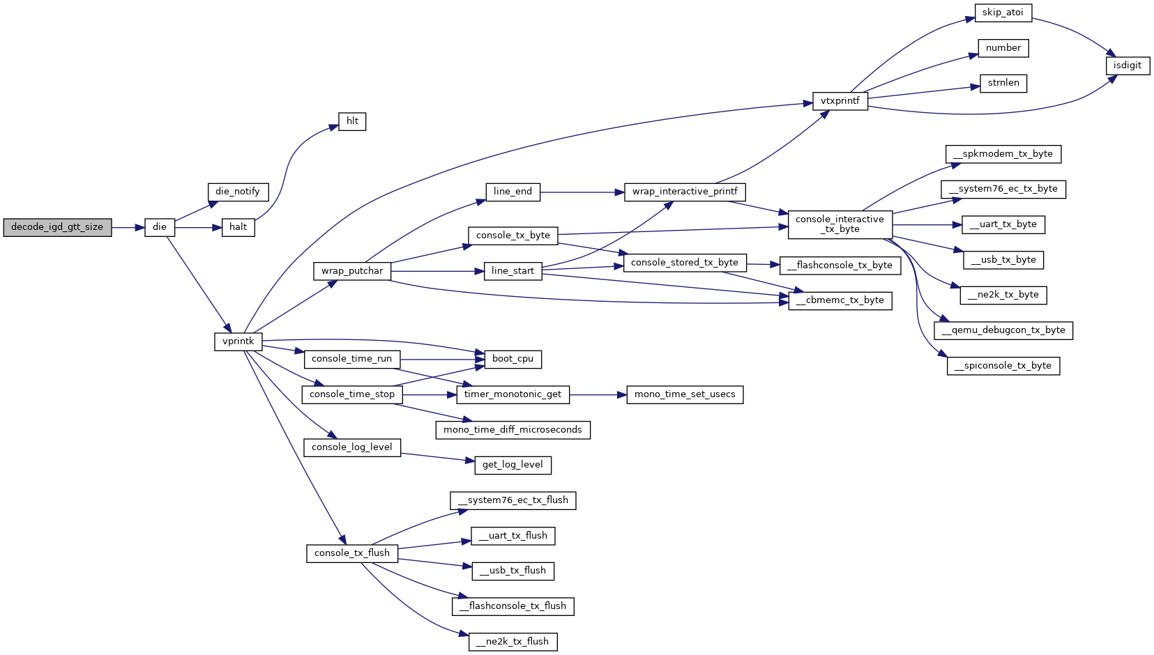
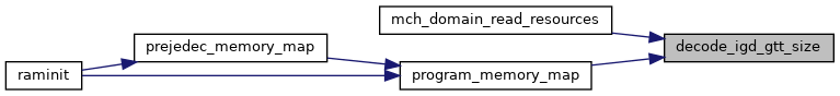
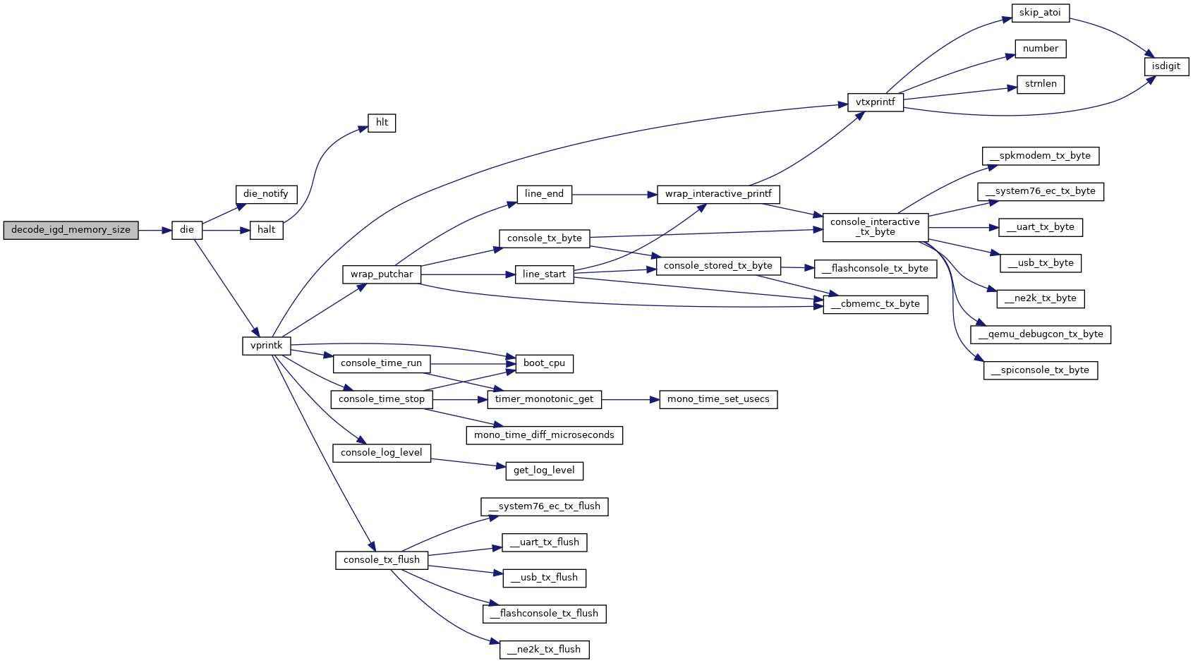
Decodes used Graphics Stolen Memory (GSM) to kilobytes.
Decodes used Graphics Stolen Memory (GSM) to kilobytes.
Definition at line 36 of file memmap.c.
References die().
Referenced by mch_domain_read_resources(), and program_memory_map().
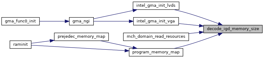
Decodes used Graphics Mode Select (GMS) to kilobytes.
Definition at line 24 of file memmap.c.
References ARRAY_SIZE, and die().
Referenced by intel_gma_init_lvds(), intel_gma_init_vga(), mch_domain_read_resources(), and program_memory_map().
Definition at line 57 of file memmap.c.
References die().
Referenced by mch_domain_read_resources().

Definition at line 191 of file raminit.c.
References BIOS_INFO, BIOS_WARNING, gm45_early_reset(), PCI_DEV, pci_read_config8(), pci_write_config8(), and printk.
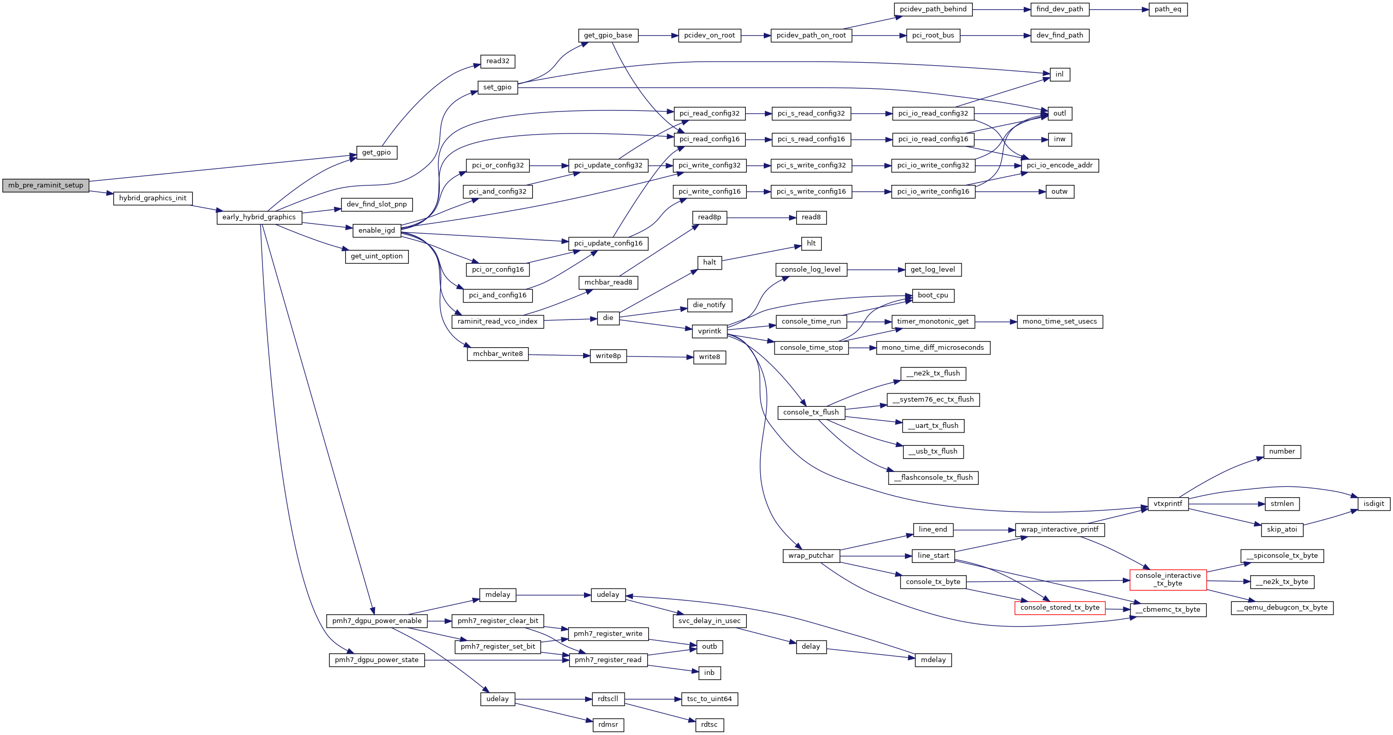
Referenced by mainboard_romstage_entry().
| u16 get_blc_pwm_freq_value | ( | const char * | edid_ascii_string | ) |
Definition at line 63 of file gma.c.
References blc_pwm_t::ascii_string, BIOS_DEBUG, BIOS_NOTICE, get_blc_values(), printk, blc_pwm_t::pwm_freq, and strcmp().
Referenced by gma_pm_init_post_vbios(), and mainboard_vbt_filename().
| int get_blc_values | ( | const struct blc_pwm_t ** | entries | ) |
Definition at line 30 of file blc.c.
References ARRAY_SIZE, and blc_entries.
Referenced by get_blc_pwm_freq_value().
Definition at line 31 of file raminit.c.
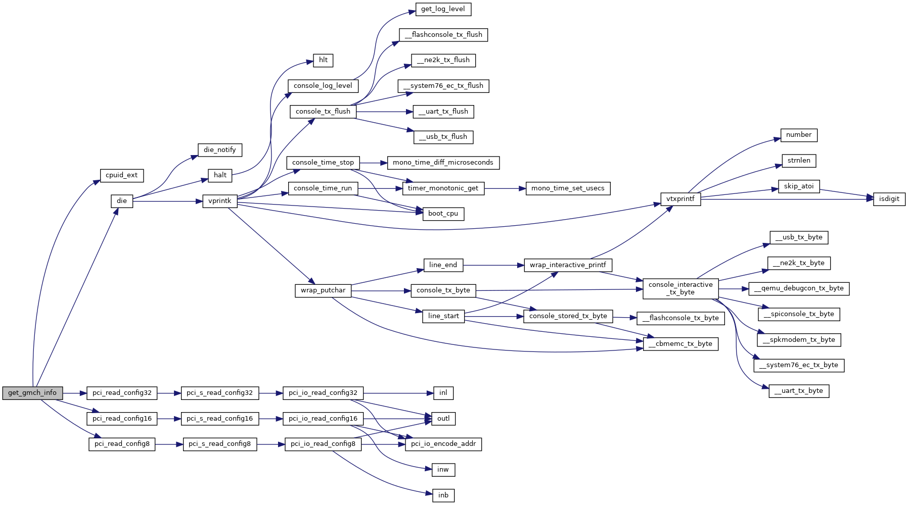
References BIOS_DEBUG, BIOS_SPEW, sysinfo::cores, cpuid_ext(), D0F0_CAPID0, die(), cpuid_result::eax, GMCH_GE45, gmch_gfx_types, GMCH_GL40, GMCH_GL43, GMCH_GM45, GMCH_GM47, GMCH_GM49, GMCH_GS40, GMCH_GS45, GMCH_PM45, GMCH_UNKNOWN, sysinfo::max_ddr2_mhz, sysinfo::max_ddr3_mt, sysinfo::max_fsb, sysinfo::max_fsb_mhz, sysinfo::max_render_mhz, PCI_CLASS_REVISION, PCI_DEV, pci_read_config16(), pci_read_config32(), pci_read_config8(), printk, STEPPING_B3, STEPPING_CONVERSION_A1, and sysinfo::txt_enabled.
Referenced by mainboard_romstage_entry().

Definition at line 18 of file romstage.c.
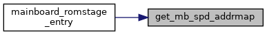
Referenced by mainboard_romstage_entry().
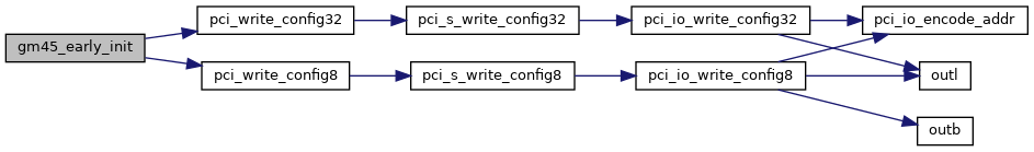
Definition at line 7 of file early_init.c.
References D0F0_DMIBAR_LO, D0F0_EPBAR_LO, D0F0_MCHBAR_LO, D0F0_PAM, D0F0_PMBASE, DEFAULT_PMBASE, PCI_DEV, pci_write_config32(), and pci_write_config8().
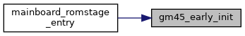
Referenced by mainboard_romstage_entry().
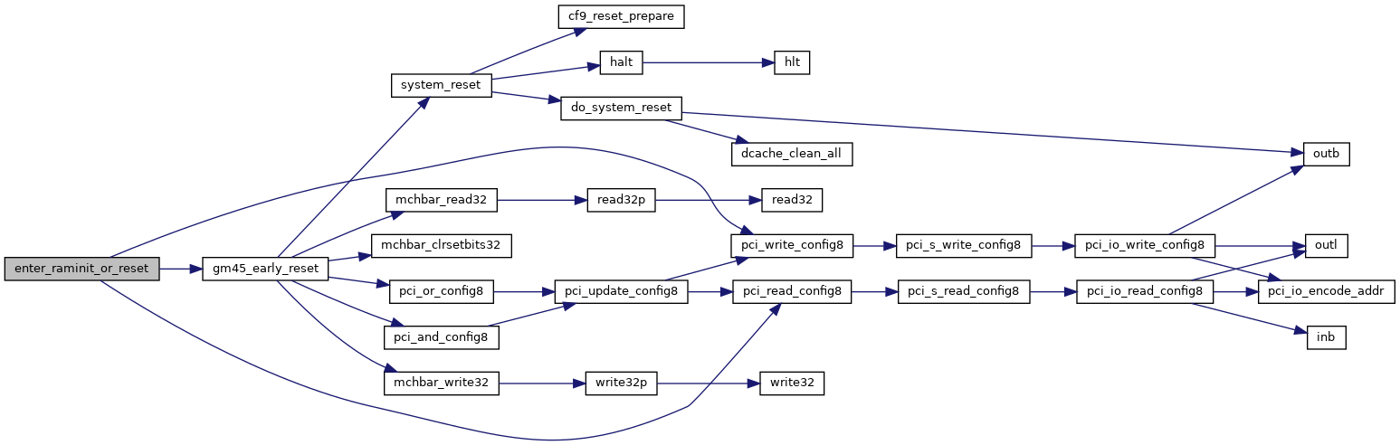
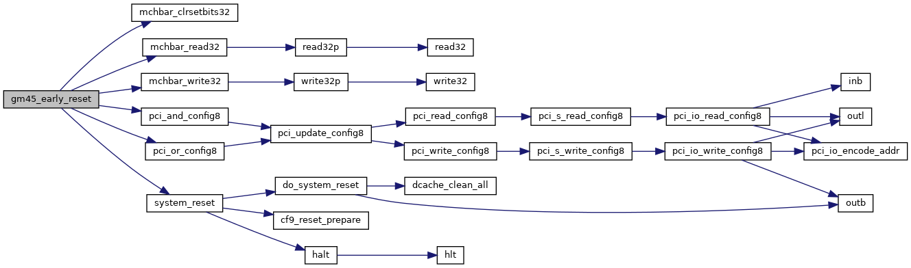
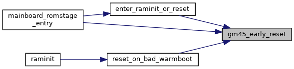
Definition at line 9 of file early_reset.c.
References ch, CLKCFG_MCHBAR, CxDRBy_BOUND_MB, CxDRBy_MCHBAR, CxDRC0_MCHBAR, CxDRC0_RANKEN, CxDRC0_RANKEN_MASK, CxDRC1_MCHBAR, CxDRC1_NOTPOP, CxDRC1_NOTPOP_MASK, CxDRC2_MCHBAR, CxDRC2_NOTPOP, CxDRC2_NOTPOP_MASK, DCC_CMD_MASK, DCC_CMD_NOP, DCC_MCHBAR, FOR_EACH_CHANNEL, mchbar_clrsetbits32(), mchbar_read32(), mchbar_setbits32, mchbar_write32(), pci_and_config8(), PCI_DEV, pci_or_config8(), RANKS_PER_CHANNEL, and system_reset().
Referenced by enter_raminit_or_reset(), mainboard_romstage_entry(), and reset_on_bad_warmboot().
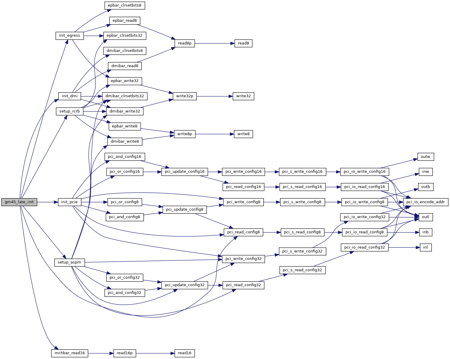
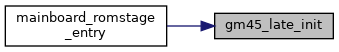
| void gm45_late_init | ( | stepping_t | stepping | ) |
Definition at line 272 of file pcie.c.
References D0F0_DEVEN, init_dmi(), init_egress(), init_pcie(), mchbar_read16(), PCI_DEV, pci_read_config8(), setup_aspm(), setup_rcrb(), stepping, and STEPPING_B2.
Referenced by mainboard_romstage_entry().
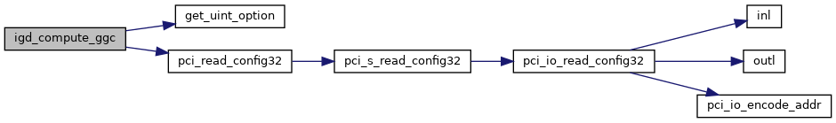
Definition at line 110 of file igd.c.
References D0F0_CAPID0, sysinfo::enable_igd, get_uint_option(), sysinfo::ggc, MAX, MIN, PCI_DEV, and pci_read_config32().
Referenced by raminit().
Definition at line 99 of file igd.c.
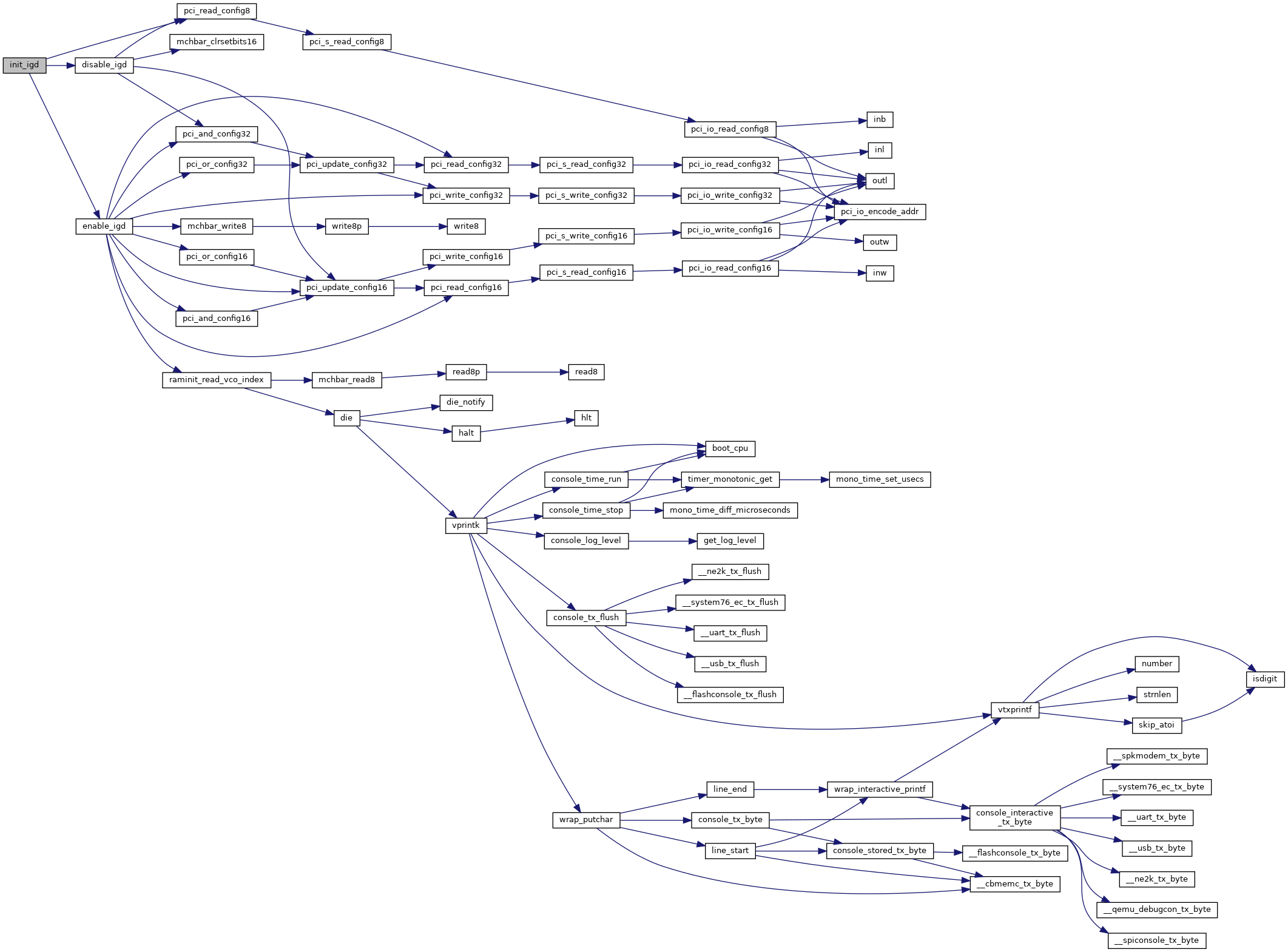
References D0F0_CAPID0, disable_igd(), enable_igd(), sysinfo::enable_igd, sysinfo::enable_peg, PCI_DEV, and pci_read_config8().
Referenced by raminit().

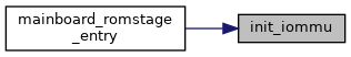
Definition at line 11 of file iommu.c.
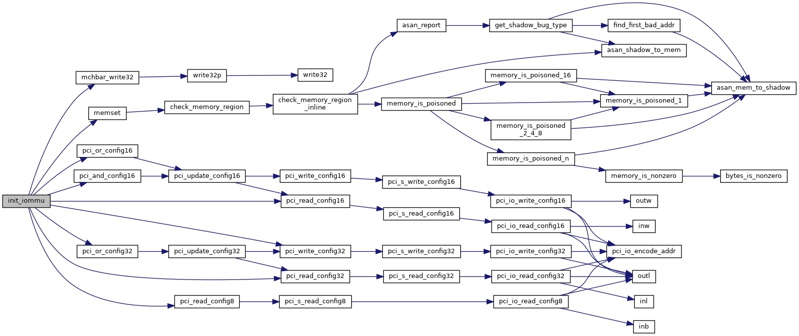
References D0F0_GGC, IOMMU_BASE1, IOMMU_BASE2, IOMMU_BASE3, IOMMU_BASE4, mchbar_setbits8, mchbar_write32(), memset(), pci_and_config16(), PCI_BASE_ADDRESS_0, PCI_CLASS_REVISION, PCI_COMMAND, PCI_COMMAND_MASTER, PCI_COMMAND_MEMORY, PCI_DEV, pci_or_config16(), pci_or_config32(), pci_read_config16(), pci_read_config32(), pci_read_config8(), pci_write_config32(), stepping, STEPPING_B2, and STEPPING_B3.
Referenced by mainboard_romstage_entry().
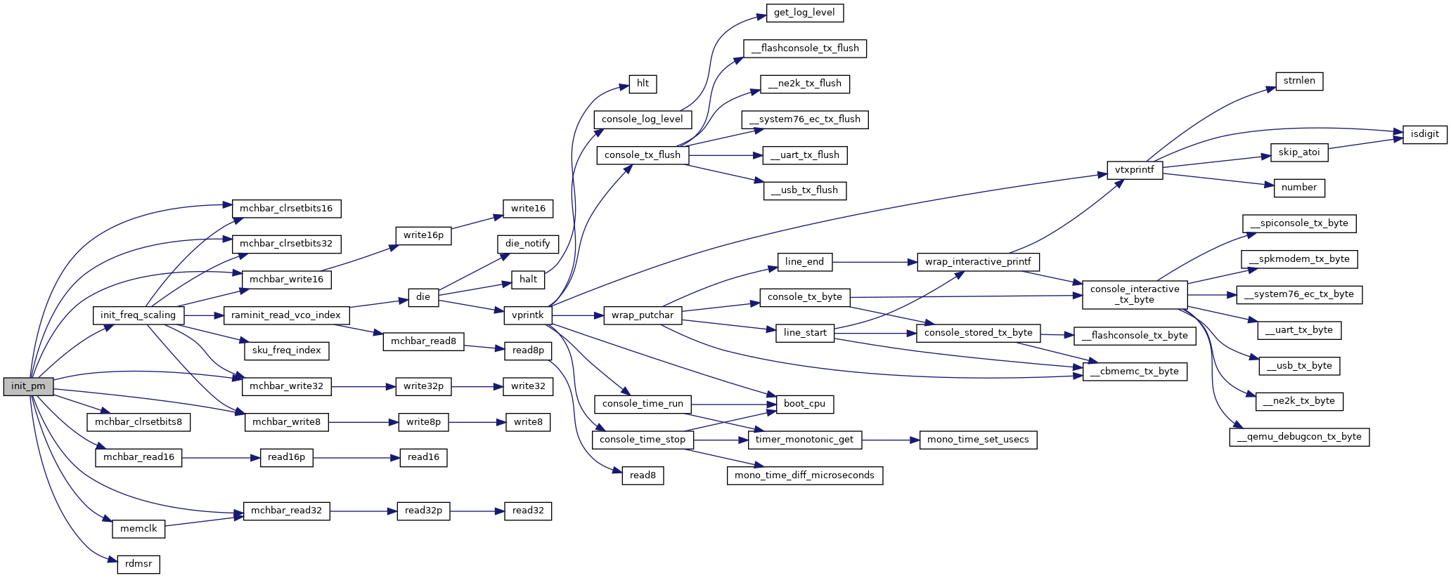
Definition at line 121 of file pm.c.
References CLKCFG_MCHBAR, sysinfo::cores, timings::fsb_clock, FSB_CLOCK_1067MHz, FSB_CLOCK_667MHz, FSB_CLOCK_800MHz, GMCH_PM45, GMCH_UNKNOWN, init_freq_scaling(), msr_struct::lo, mchbar_clrbits16, mchbar_clrbits32, mchbar_clrbits8, mchbar_clrsetbits16(), mchbar_clrsetbits32(), mchbar_clrsetbits8(), mchbar_read16(), mchbar_read32(), mchbar_setbits16, mchbar_setbits32, mchbar_setbits8, mchbar_write16(), mchbar_write32(), mchbar_write8(), timings::mem_clock, MEM_CLOCK_667MT, memclk(), MSR_EXTENDED_CONFIG, rdmsr(), sysinfo::selected_timings, stepping, STEPPING_B0, STEPPING_B1, STEPPING_B2, STEPPING_B3, and STEPPING_CONVERSION_A1.
Referenced by mainboard_romstage_entry().

Definition at line 43 of file romstage.c.
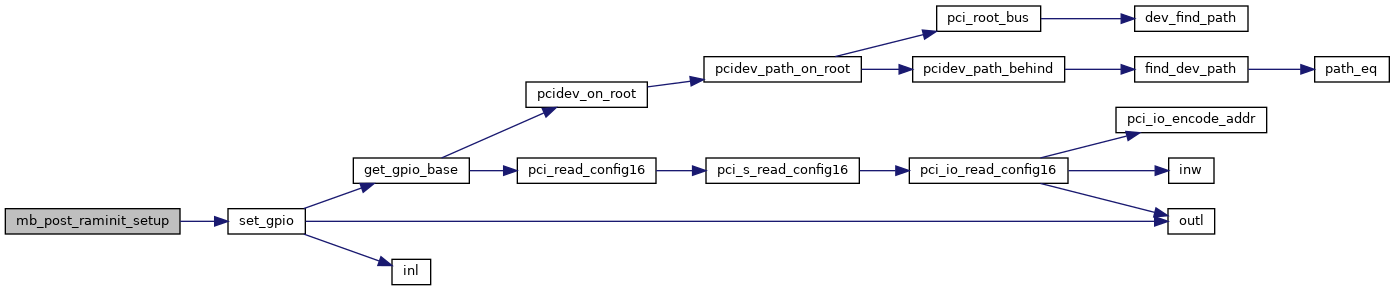
References GPIO_LEVEL_LOW, and set_gpio().
Referenced by mainboard_romstage_entry().
Definition at line 24 of file romstage.c.
References BIOS_DEBUG, CONFIG, sysinfo::enable_igd, sysinfo::enable_peg, get_gpio(), hybrid_graphics_init(), and printk.
Referenced by mainboard_romstage_entry().
Definition at line 18 of file romstage.c.
Definition at line 1691 of file raminit.c.
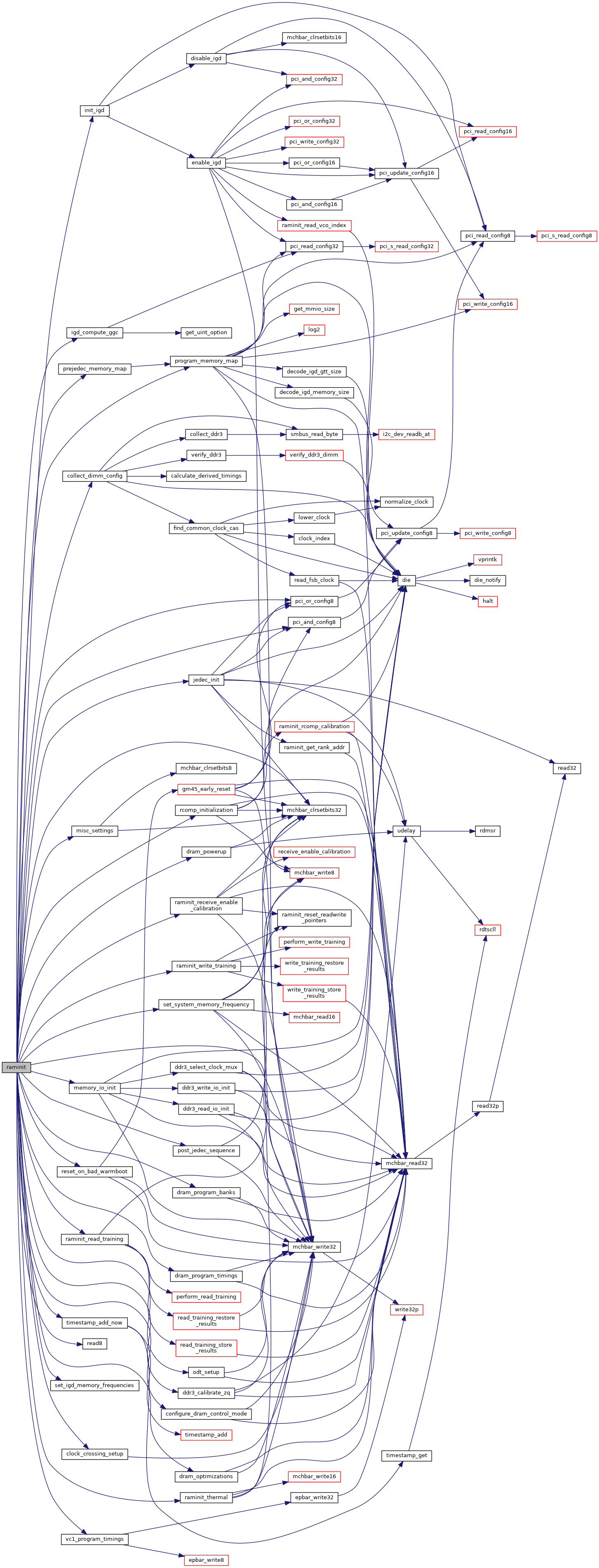
References ch, clock_crossing_setup(), collect_dimm_config(), configure_dram_control_mode(), sysinfo::cores, CxDCLKDIS_ENABLE, CxDCLKDIS_MCHBAR, CxDRT3_MCHBAR, CxDRT5_MCHBAR, DCC_MCHBAR, DDR2, DDR3, ddr3_calibrate_zq(), sysinfo::dimms, dram_optimizations(), dram_powerup(), dram_program_banks(), dram_program_timings(), FOR_EACH_POPULATED_CHANNEL, timings::fsb_clock, sysinfo::ggc, igd_compute_ggc(), init_igd(), jedec_init(), mchbar_clrsetbits32(), mchbar_read32(), mchbar_setbits32, mchbar_setbits8, timings::mem_clock, MEM_CLOCK_1067MT, memory_io_init(), misc_settings(), odt_setup(), pci_and_config8(), PCI_DEV, pci_or_config8(), post_jedec_sequence(), prejedec_memory_map(), program_memory_map(), raminit_read_training(), raminit_receive_enable_calibration(), raminit_thermal(), raminit_write_training(), rcomp_initialization(), read8(), reset_on_bad_warmboot(), sysinfo::selected_timings, set_igd_memory_frequencies(), set_system_memory_frequency(), sysinfo::spd_type, timestamp_add_now(), TS_INITRAM_END, TS_INITRAM_START, sysinfo::txt_enabled, and vc1_program_timings().
Definition at line 1660 of file raminit.c.
References CxDRBy_BOUND_MASK, CxDRBy_BOUND_SHIFT, CxDRBy_MCHBAR, and mchbar_read32().
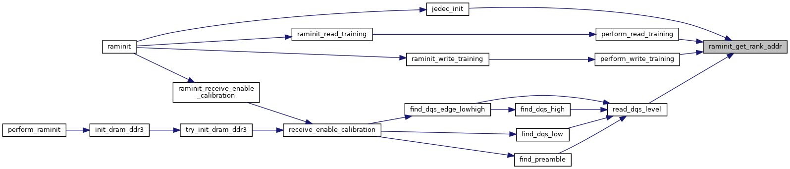
Referenced by jedec_init(), perform_read_training(), perform_write_training(), and read_dqs_level().

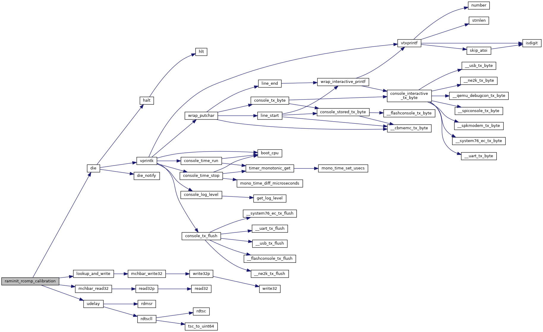
| void raminit_rcomp_calibration | ( | stepping_t | stepping | ) |
Definition at line 164 of file raminit_rcomp_calibration.c.
References ddr3_lookup_schedule, die(), lookup_and_write(), mchbar_clrbits32, mchbar_read32(), mchbar_setbits32, PULL_DOWN, PULL_UP, stepping, STEPPING_CONVERSION_A1, and udelay().
Referenced by rcomp_initialization().

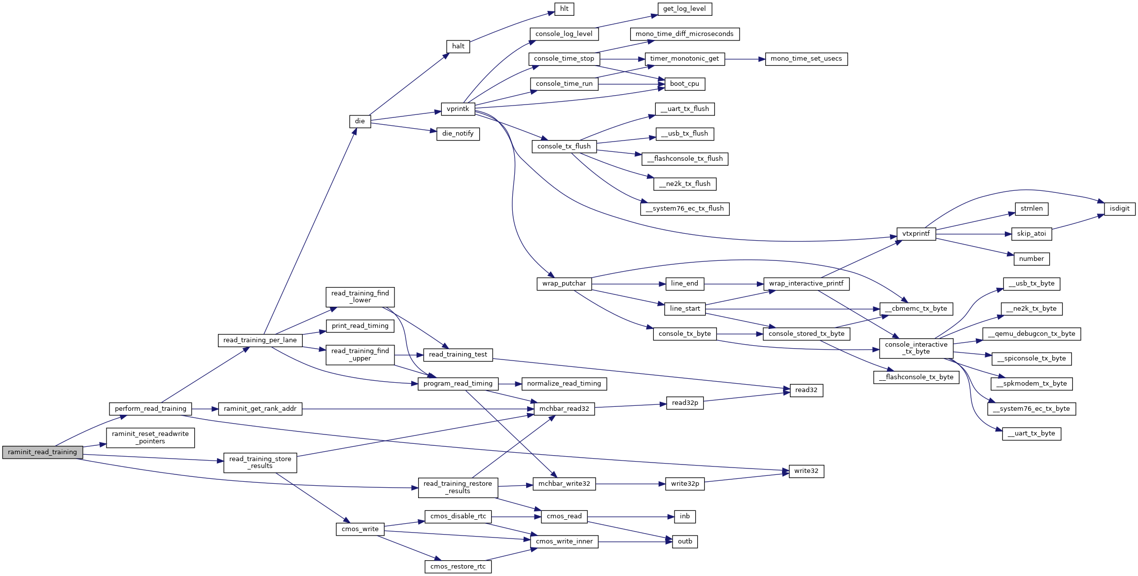
| void raminit_read_training | ( | const dimminfo_t * | dimms, |
| int | s3resume | ||
| ) |
Definition at line 265 of file raminit_read_write_training.c.
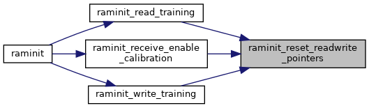
References perform_read_training(), raminit_reset_readwrite_pointers(), read_training_restore_results(), and read_training_store_results().
Referenced by raminit().

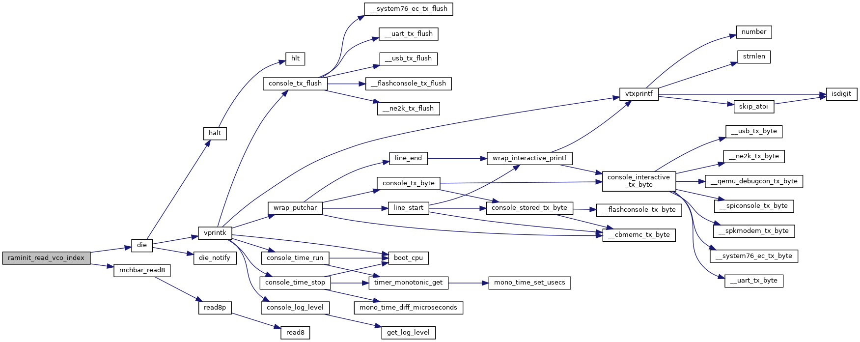
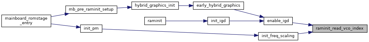
| int raminit_read_vco_index | ( | void | ) |
Definition at line 733 of file raminit.c.
References die(), HPLLVCO_MCHBAR, mchbar_read8(), VCO_2666, VCO_3200, VCO_4000, and VCO_5333.
Referenced by enable_igd(), and init_freq_scaling().
| void raminit_receive_enable_calibration | ( | const timings_t * | timings, |
| const dimminfo_t * | dimms | ||
| ) |
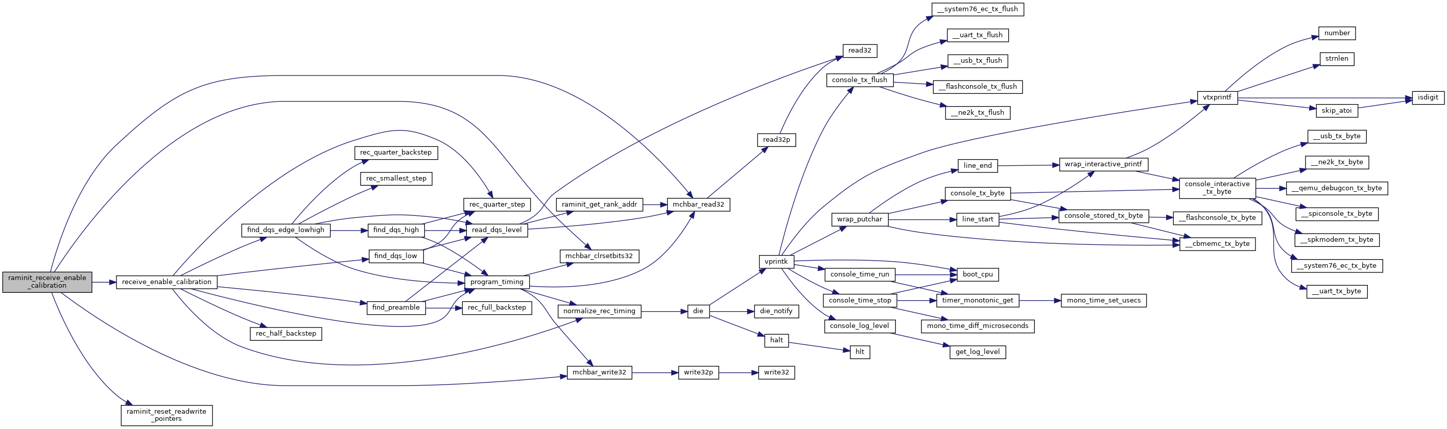
Definition at line 262 of file raminit_receive_enable_calibration.c.
References bytelane_map, dimminfo_t::card_type, ch, CxRECy_MCHBAR, FOR_EACH_POPULATED_CHANNEL, mchbar_clrbits32, mchbar_clrsetbits32(), mchbar_read32(), mchbar_setbits32, mchbar_write32(), raminit_reset_readwrite_pointers(), and receive_enable_calibration().
Referenced by raminit().

Definition at line 1677 of file raminit.c.
References mchbar_clrbits32, and mchbar_setbits32.
Referenced by raminit_read_training(), raminit_receive_enable_calibration(), and raminit_write_training().
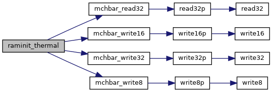
Definition at line 10 of file thermal.c.
References CHANNEL_MODE_DUAL_INTERLEAVED, CHIP_CAP_1G, CHIP_CAP_2G, CHIP_CAP_512M, dimminfo::chip_capacity, CHIP_WIDTH_x16, CHIP_WIDTH_x8, CxDTAEW, CxDTC, CxDTPEW, CxGTC, CxGTEW, sysinfo::dimms, FOR_EACH_POPULATED_CHANNEL, timings::fsb_clock, FSB_CLOCK_1067MHz, FSB_CLOCK_667MHz, FSB_CLOCK_800MHz, GMCH_GM49, GMCH_PM45, GMCH_UNKNOWN, mchbar_clrbits16, mchbar_read32(), mchbar_setbits32, mchbar_write16(), mchbar_write32(), mchbar_write8(), timings::mem_clock, MEM_CLOCK_1067MT, MEM_CLOCK_667MT, MEM_CLOCK_800MT, sysinfo::selected_timings, width, and x.
Referenced by raminit().

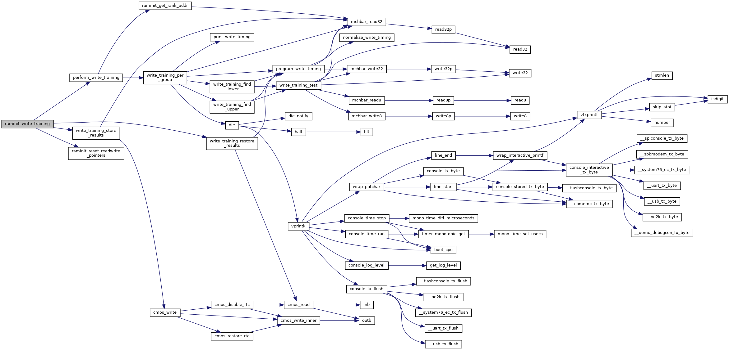
| void raminit_write_training | ( | const | mem_clock_t, |
| const dimminfo_t * | dimms, | ||
| int | s3resume | ||
| ) |
Definition at line 634 of file raminit_read_write_training.c.
References MEM_CLOCK_1067MT, perform_write_training(), raminit_reset_readwrite_pointers(), write_training_restore_results(), and write_training_store_results().
Referenced by raminit().